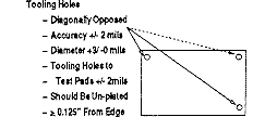
Place two (or three) diagonally opposed, unplated tooling holes as far apart as possible with a tolerance between holes of ±0.002" to ensure correct fixture placement. Tooling pin flex can be minimized by using at least 0.125" diameter holes. Tooling hole diameters should be maintained to within 0.003"/-0.000". Solder contamination and plating thickness variation problems can be prevented by keeping tooling holes free of plating.
Minimum Optimal Test Pad Positioning and Size
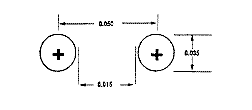
The tolerance from a test pad to tooling hole should be held to ±0.002". Clear access to test pads is vital. Ideally, test pads should be provided on each node. If possible, always place test pads on one side of the board to minimize the likelihood of more expensive double-sided fixtures. Test pads should be round, and nominally 0.035" in diameter with pad-to-pad accuracy of ±0.003".
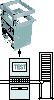
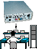
PCB test access is typically accomplished through a bed-of-nails fixture, or higher performance short-wire fixtures. On automated manufacturing production lines where boards arrive at the ATE via conveyors, mechanically actuated fixtures are used.
Mechanical board handlers may need as much as 0.138" clearance from components and 0.125" clearance from test pads to provide room for conveyor rails.
Test pads should also be located at least 0.125" from the board edge because, pick and place systems and handlers require access to the board edges.
Test pad spacing should be 0.100"whenever possible, 0.050" at a minimum. Test Electronics can probe centers as close as 0.015", but these small probes are expensive and do not have the durability of the larger probes.
Test pads on the component side of the board should have at least 0.040' clearance from components to avoid damage to either the probe or the part.
Proximity to Signal Source
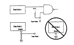
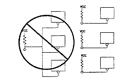
Place test points as close as possible to the signal source to minimize the electrical impact of the tester on the circuit board. Place several test pads on the VCC and ground lines to assure a more even power distribution. Keep in mind that heavy backdrive currents can shift ground potentials.
|
Accessibility Guidelines for SMT Boards
|
|
Test pads should be 0.015 to 0.040 inches in
diameter.
|
Based on generally accepted test fixture/PCB
manufacturing tolerances, the SMD probe requires a test pad of this size for
repeated tip-to-target accuracy. Naturally, the larger the target, the greater
probability of hitting it
|
|
Coat test pads with conducive non-oxidizing
material.
|
Test pads should be solder coated or coated with a
non-oxidizing material such as gold. Solder oxides are easily penetrated with
most sharp tip styles, ensuring good electrical integrity.
|
|
Probe test pads or vias, not components or component
leads.
|
Probing a component lead may force a broken or cold
solder joint to make contact and appear good.
|
|
Provide accurate tooling pins.
|
The tooling pin location is key to fixture/PCB
alignment Tolerance from the DUT to the datum to the test pad should be ±0.002
in.
|
|
Place tooling holes as far apart as possible.
|
Tooling holes on the PCB should be as far apart as
possible, diagonally placed, with a tolerance between holes of ±0.002 in. A
0.125 in. or larger tooling pin will help maintain stability and PCB/fixture
alignment. Tooling hole diameter tolerance should be within +0.003/ -0.000 in.
|
|
Minimize use of tall components.
|
SMT boards with component height greater than 0.35
in. are difficult to probe, requiring cutouts or relief in the probe plate. When
possible, extend test pads 0.1 in. away from tall components to allow for
milling tolerances.
|
|
Don't crowd test pads.
|
Leave a 0.018 in. unpopulated area around each test
pad to minimize shorting during worst-case tolerance scenarios.
|
Device pins (through-hole), test pads, connectors, and vias can be used to allow adequate test access. For PCBs using Surface Mount Technology (SMT), test pads must be used since probing may damage the leads and open solder connections may be temporarily connected when the probe presses the leads onto the trace surface.
Test pad diameters should be between 0.015" to 0.040" nominally 0.035" when using standard 100-mil, 75-mil, or 50-mil test probes and should have an adequate solder surface to ensure reliable probe contact. 30-mil to 15mil probes are more fragile, more expensive, and less reliable. During test fixture layout, every attempt should be made to minimize the need for 30-mil to 15mil probes. For greater accessibility on fine-pitch devices, test pads should be staggered to allow 50-mil spacing.
When probing connectors, it is typical to probe the solder side of a through hole mount with a crown shaped test probe tip. Test access can be obtained through the connectors and the connectors can be tested. Special test probe tip styles are available to fit a wide variety of female connectors. Male connectors can be tested using special shrouds with cupped style probe tips up inside the shrouds.
Where via probing is necessary, soldering or gold plating the vias provides a good probing surface. Vias must not be solder masked as this will insulate and block probe contact.
Balance Probe Density, Vacume Only
One of the great advantages of mechanical fixtures is that they do not require a balance of probe density. For vacume fixtures only. To ensure PCB coplanarity, increase probing precision, and minimize component damage due to PCB flexing, test pad density should not exceed 12 per square inch (8 oz. probes). Excessive probe density may hinder proper sealing of vacuum fixtures. In every case, probing densities must be carefully planned to achieve the best testability.
Tall PCB components (> 0.35") necessitate milling the test fixture for extra clearance. As a precaution to avoid damage to the component and to prevent probe-induced shorts, test pads should not be placed within 0.1" of such components.
Electrical Design Considerations
There are several fundamental design considerations that can have a major impact on a PCB's testability and, therefore, its cost
While the current handling capacity of standard probes is 1 amp, a practical limitation of 1/2 amp will guarantee more efficient probe performance and reliable power distribution. Power distribution should take place across the entire board with at least three test points for the first amp and another test point for an additional 1/2 amp. Additional test points must be included for power supply sense lines, as well as grounds and returns, especially in digital logic testing. Any PCB changes, i.e., jumpers or components on the probe surface, must be positioned carefully so as not to interfere with probe access.
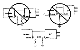
Typically on-board clocks must be disabled to effectively test the rest of the circuit Clock sources must be controllable from the tester.
External control or output lines must not be tied directly to ground or to the VCC. Otherwise, it's impossible to use available test library elements easily, leading to a more complex and more costly test routine.
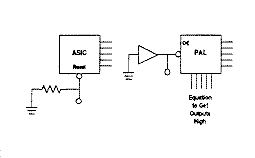
Separate Resets and Enables
Similarly, separate reset, control, and enable lines must not be tied through a common resistor as this prohibits independent testing of each device.
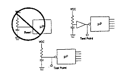
Make reset points accessable.
Keep Resets and Enables Separate
Power-on reset circuits must be able to be driven by the tester to achieve a known circuit state.
Make sure that the reset line to an ASIC or the output enable lines on a PAL are accessible to the tester. You may alternatively provide a simple equation that can be entered by the tester to set the outputs of a PAL to a known state.
All unused pins must be nailed with a test pin to ensure that faults associated with these unused pins do not propagate through the circuit.
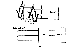
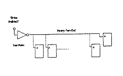
Drive High Powered Devices by the Inputs
Many times, lengthy test backdriving of a power device, such as a 244, can lead to device destruction due to excessive heat build-up. Driving the inputs rather than driving the outputs should be used whenever possible to avoid excessive backdrive on power devices with heavy fan-out capabilities.
Serial Chains Waste Test Time
Long serial chains also require special handling to prevent test times from becoming excessive. Breaking the chain with test access generally slashes the test time by orders of magnitude.
Flash EPROMS require special testability consideration. Do not program the protection bit until after the test Do not use Hardware Fault Insertion as it might re-program the device. Program first... then verify.
An on-board battery requires a jumper because it is difficult to detect shorts around a battery
A ball grid array essentially has very limited access to its nodes. This often requires a form of cluster test in which a EGA is tested in conjunction with other devices that define a more testable functional block.
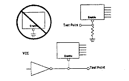
Many analog and mixed signal devices can react adversely to the electrical loading of tester and fixture. Test points need to be buffered or placed very close to the signal source; alternatively, the device can be tested as a cluster.
It's there...but can I probe it?
that are accessible or not and those that are probeable or not. Accessible nodes might not be probeable due to tester loading on the circuit An inaccessible node might be probeable through indirect means such as Boundary Scan virtual nail. Unprobeable and inaccessible nodes are either untestable or require alternative means such as cluster test, etc.
Many innovative testing strategies are being introduced that will enhance the likelihood of testability. These include the adoption of Boundary Scan designs, automated test model development, and analog testing of digital opens.
The Testability Challenge
Regardless of the trends in system test capability, the basic challenge for test engineers is not to change the design but rather to make the designer a believer in testability.